Semiconductor Weekly — Mar 10, 2026
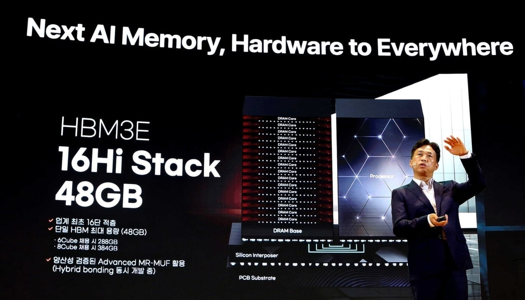
Photo: lyceumnews.com
Week of March 10, 2026
The Big Picture
The AI chip buildout is still accelerating — TSMC's 2nm node is in volume production, the $796 billion 2025 market is officially in the books, and Nvidia in early March 2026 announced $4 billion in investments to lock up the photonics supply chain. But the bottlenecks have migrated. It's no longer about getting a GPU die to tape out; it's about packaging it, stacking memory on top of it, wiring light through it, and finding the substrate to hold it all together — while memory prices spike, export controls tighten on yet another layer of the stack, and China's software engineers quietly prove they can do more with less silicon than anyone assumed.
This Week's Stories
Apple and Nvidia Are Elbowing Each Other for TSMC's Most Advanced Node
The most important fab fight of 2026 is playing out right now across TSMC's Hsinchu and Kaohsiung campuses, and it involves the world's two most valuable technology companies competing for the same wafers.
TSMC's N2 process — its 2-nanometer node — entered high-volume manufacturing in late 2025. N2 introduces Gate-All-Around (GAA) nanosheet transistors, replacing the FinFET architecture that dominated advanced chips for over a decade. Think of it as redesigning the tiny on/off switch at the heart of every chip from scratch: the gate material now wraps around the current-carrying channel on all four sides instead of three, giving better control at smaller dimensions. The result is about a 30% reduction in power for equivalent speed, or roughly a 10–15% performance boost for equivalent power.
The problem is there isn't enough of it. TSMC targets over 100,000 wafer starts per month in 2026, but combined demand from Apple, Nvidia, Qualcomm, MediaTek, and Amazon exceeds that. Apple locked in early, securing roughly 50% of N2 capacity for 2026. But Nvidia is pushing back hard. Supply chain sources say Nvidia became TSMC's largest customer in at least one quarter of 2025 and is expected to hold that position through most of 2026 — the first time in a decade Apple hasn't been the dominant buyer on a new node.
This isn't just a wafer story. Nvidia's simultaneous moves to lock photonics capacity and CoWoS advanced packaging slots mean it's competing with Apple across three dimensions at once: wafer starts, packaging, and interconnect. Everyone else — Qualcomm, AMD, MediaTek — is essentially waiting in the lobby. If N2 yields improve faster than expected, the crunch eases. If they don't, the queue gets longer.
Three Memory Giants Are Racing to Stack 16 Chips on Top of Each Other
High-Bandwidth Memory (HBM) is the speed layer that sits right next to the GPU die in every AI accelerator — a tower of individual DRAM chips bonded together and connected through thousands of tiny vertical wires called through-silicon vias. Today's chips use 12-layer stacks. Nvidia wants 16. And it wants them by Q4 2026.
The technical challenge is deceptively brutal. Current 12-layer HBM uses wafers thinned to about 50 micrometers — roughly the width of a human hair. Going to 16 layers means shaving each wafer down to around 30 micrometers without cracking it, across hundreds of thousands of units, at production volume. SK Hynix, Samsung, and Micron have all begun full-scale development.
The competitive dynamics are sharpening fast. SK Hynix controls roughly 60% of the HBM market as of 2025 and is effectively sold out through 2026, with roughly 20% price increases on current-gen HBM3E through early 2026. Korean outlets now report that Nvidia has chosen Samsung and SK Hynix as primary HBM4 suppliers for its flagship Rubin platform, assigning Micron to a mid-range variant. If confirmed, that reshapes pricing leverage and qualification timelines for the entire Rubin ramp.
SK Hynix also quietly hinted that HBM4 sampling is moving into mid-2026 — earlier than public roadmaps suggest. If those samples pass early integration tests with CoWoS packaging, late-2026 Rubin launches become more plausible. The winner of the 16-Hi race captures the supply chain for Nvidia's next GPU generation. The structural constraint isn't ambition — it's physics.
AI Is Eating Your PC's Memory — Literally
There's a reason the RAM in your next laptop is going to cost more, and it's not inflation. It's a decision being made in cleanrooms in South Korea.
Memory makers have shifted manufacturing capacity away from the conventional DRAM and NAND used in smartphones and PCs toward high-margin HBM and server DDR5 for AI data centers. Producing a gigabyte of HBM takes three to four times as many wafers as producing a gigabyte of DDR5 today — so every wafer allocated to an Nvidia GPU's memory stack is a wafer denied to a mid-range smartphone or consumer SSD. IDC expects 2026 DRAM and NAND supply growth of just 16% and 17% year-on-year (2026 vs. 2025) — well below historical norms.
The spot market is already screaming. TrendForce data shows NAND flash spot prices climbed 14.7% in a single week through early March 2026, with DRAM spots running above contract prices before Q2 2026 negotiations have even started. TrendForce revised its Q1 2026 forecast for conventional DRAM contract prices up to +90–95% quarter-over-quarter (Q1 2026 vs. Q4 2025); PC DRAM prices are expected to at least double quarter-over-quarter in Q1 2026. DigiTimes reports that DRAM spot quotes were changing hourly in early March 2026 for some buyers, creating a brutal environment for smaller hardware companies that can't execute instant purchase orders.
Samsung is accelerating the squeeze by retiring its last 2D NAND line to repurpose tooling for higher-value DRAM products, a move announced in early 2026. OEM procurement teams building bills of materials for H2 2026 devices should be stress-testing DRAM cost assumptions now — not next quarter.
Nvidia Puts $4 Billion on Photonics to Avoid the Next AI Bottleneck

If you run AI clusters, your next constraint isn't GPUs — it's the plumbing between them.
Nvidia announced $2 billion investments each in U.S. photonics suppliers Lumentum and Coherent, alongside multibillion-dollar long-term purchase commitments for silicon-photonics components and optical networking gear. The deals include capacity guarantees and U.S.-based R&D and manufacturing expansion, effectively pre-allocating a large chunk of future high-end optics output to Nvidia's platforms.
The logic is straightforward: electrical copper links are already the power and cost wall for 800G/1.6T switches and GPU clusters. Moving to in-package and short-reach optics — using light instead of electrons to shuttle data between chiplets — is how you keep scaling without melting the rack. Nvidia's networking business has already surpassed $31 billion in annual revenue as of 2025, making it arguably the world's largest pure-play networking vendor by AI-focused sales.
For the rest of the ecosystem — switch ASIC vendors, other GPU makers, hyperscalers — Nvidia just turned high-end optics into a strategic resource, not a commodity line item. Optical module capacity, photonics test gear, and packaging flows are now first-order procurement items.
Washington Loosens One Hand and Tightens the Other on Chip Exports
The U.S. export control posture crystallized over the past two months — and it's more nuanced than either hawks or industry lobbyists wanted.
In January 2026, BIS revised its license review policy for exports of certain semiconductors to China, shifting from a presumption of denial to case-by-case review for chips like the Nvidia H200. The conditions are strict: applicants must prove exports won't reduce capacity available to U.S. customers, demonstrate the Chinese buyer has compliance procedures, and submit products for independent third-party testing. The same week (mid-January 2026), a 25% tariff was applied to those same chips.
BIS also shut a door: the Validated End User program that let select foreign fabs export U.S.-origin goods to China license-free was terminated. Former participants have 120 days to apply for new licenses — and BIS does not intend to approve capacity expansions or technology upgrades at those fabs. That's a slow freeze on foreign-owned China operations (Samsung, SK Hynix, and others with cleanrooms there) that will quietly constrain them over time.
Then on March 6, 2026, BIS posted a draft rule targeting AI chip design software — the EDA toolchains used to design sub-3nm accelerators — with a public comment window. If that advances, it directly affects Cadence and Synopsys tooling access and could slow Chinese fabless designers' ability to use the most advanced design kits.
And on March 8, 2026, media reported the U.S. targeted certain substrates and materials used in HBM modules, making shipments to specific Chinese entities license-controlled. Adding HBM substrates to the control list creates a geopolitical single point of failure for the entire HBM packaging chain. The net effect: selling H200-class chips to China is theoretically possible but operationally expensive, and the control perimeter is expanding from silicon into software, substrates, and materials.
New Products & Launches
China's Qiwang S3 inference GPU from Hangzhou-based Sunrise is China's first GPU to adopt LPDDR6 memory, supporting flexible multi-precision computing from FP16 down to FP4. In large-model inference scenarios including DeepSeek V3/R1 deployments, it reduces per-token inference cost by approximately 90% compared with its predecessor (TrendForce, Feb 2026). Not competing with Nvidia on training — but inference is the actual market being contested.
Iluvatar CoreX's Tianxuan architecture launched alongside the company's Hong Kong Stock Exchange listing — the company says it's China's first to achieve mass production of general-purpose GPUs for both training and inference, having delivered over 52,000 GPUs to 290+ customers to date (early 2026). Its roadmap targets surpassing Nvidia's Rubin architecture by 2027.
Intel's 18A process is now accepting external customers as of March 2026, with the company reporting inbound interest and improving yields. The short-term effect isn't a flood of wafer starts — it's a strategic lever that gives big chip buyers another card to play when negotiating TSMC commitments.
⚡ What Most People Missed
CoWoS is still the load-bearing wall. TSMC's advanced packaging capacity is fully booked through 2026 (as of March 2026), with CoWoS-L lead times reportedly stretching beyond 18 months. ABF substrates — the thin insulating films used in advanced packages — are also constrained. Even qualified wafers sit idle without packaging slots, which is why accelerator lead times remain multi-quarter despite logic capacity additions.
Materials inflation is the quiet tax on everything. Mitsubishi Gas Chemical announced around 30% price increases on copper-clad laminates and prepregs in late February 2026, citing copper and resin constraints. Vishay issued emergency price hikes in late February 2026 on MOSFETs and power ICs. Tantalum and high-reliability passives are being repriced in bilateral deals. The packaging, HBM, and interposer supply chains all depend on a small set of substrate suppliers whose lines are much harder to scale than wafer fabs.
Alibaba proved you can run AI on 82% fewer GPUs — and the real story is what comes next. Alibaba Cloud's Aegaeon pooling system (reported March 2026) virtualizes GPU access at the token level, letting 213 H20 GPUs do the work of 1,192 in its tests. The techniques — token-level scheduling, dynamic model sharing, disaggregated decoding — may be applied to other accelerators such as Huawei Ascend chips or domestic alternatives. This is software paving the road for domestic hardware, and if other Chinese hyperscalers publish similar numbers, GPU demand models for China need rewriting.
SK Hynix pulled DRAM capacity forward. Trial runs at its Yongin complex moved into February–March 2026, and its Cheongju M15X fab is targeting 55,000–60,000 wafers per month by year-end 2026. That's an aggressive calendar pull-in for a greenfield site — but most of that capacity is pre-allocated to hyperscalers, so consumer DRAM relief isn't coming soon.
8-inch fabs are quietly filling up again. Global 200mm foundry utilization is projected to rebound to 85–90% in 2026, driven by power-management ICs for AI servers, EVs, and industrial automation. The mature-node capacity that everyone forgot about while chasing N2 is becoming strategically scarce — expect another round of "how is a 0.18 µm chip gating a $60,000 product?" conversations by 2027.
📅 What to Watch
- If TSMC's February 2026 revenue (reported mid-March 2026) continues above roughly $10 billion monthly, it would indicate N2 demand is absorbing ramp costs faster than expected and increase the odds TSMC reallocates wafers toward N2 customers, easing CoWoS and HBM package lead times six months out.
- If Samsung's Q1 2026 earnings include specific 16-Hi HBM4 qualification timelines, it directly signals Nvidia's Rubin production schedule; vague language means Samsung is still behind SK Hynix.
- If Chinese hyperscaler GPU capex guidance comes in below consensus, it would imply Aegaeon-style efficiency gains are already being implemented at scale, reducing expected GPU and HBM order volumes from China and compressing supplier pricing power over the coming two quarters.
- If BIS's draft rule on AI chip design software (posted March 6, 2026) advances past the comment period, Cadence and Synopsys face real constraints on China-facing EDA licensing — watch for GSA or SEMI formal comment filings as the early warning.
- If India's packaging plants (Micron, Tata, Kaynes, CG Power) begin commercial operations on schedule, they would provide regional ABF substrate and assembly capacity to relieve some hyperscaler lead times and lower shipping risk; any delay keeps global back-end supply concentrated in China/ROK/Taiwan.
- If Rapidus's second 2nm fab in Japan hits tool move-in milestones, Asia-Pacific capacity diversification shifts from aspiration to a concrete alternative — watch for equipment vendor disclosures naming the site.
This week in three images: Apple and Nvidia in a cage match over wafers thinner than a human eyelash; Korean engineers shaving silicon to 30 micrometers without cracking it, because Nvidia asked nicely; and Alibaba's software team proving that the most powerful GPU optimization is not buying GPUs.
The real punchline is that Mitsubishi Gas Chemical — a company most chip architects couldn't pick out of a lineup — announced around a 30% price increase in late February 2026 on the laminate that holds your $30,000 HBM module together, and nobody's writing the headline.
Until next week. —Semiconductor Weekly