Semiconductor Weekly — Apr 22, 2026
Photo: lyceumnews.com
Week of April 22, 2026
The Big Picture
Korea is running two parallel dramas that together explain the state of the industry. SK Hynix poured concrete on a $13 billion dedicated HBM packaging plant — the largest back-end investment in Korean history — while Samsung's unions prepare to mass 30,000+ workers at Pyeongtaek on April 23 ahead of a potential 18-day strike that could cost up to 30 trillion won. One memory giant is compounding its lead; the other is fighting a talent war it appears to be losing. Meanwhile, under the noise, the spot market is quietly drifting lower even as contract memory prices are guided up 60–75% for Q2 — and that divergence is the tell.
What Just Shipped
- 192GB SOCAMM2 (SK Hynix): Mass production began April 19 of the first server memory module built for Nvidia's Vera Rubin platform — more than double the bandwidth and about 75% better power efficiency versus conventional RDIMM, per SK Hynix's announcement.
- Automotive Wi-Fi 7 Communication Module (LG Innotek): Supply deal signed April 20 to bring Wi-Fi 7 bandwidth into production vehicles.
- P&T7 Groundbreaking (SK Hynix): Construction officially began on the $13 billion Cheongju HBM packaging plant, with a wafer-test line targeted for October 2027.
- 2nm PDK Release Plan (Rapidus): Japan's NEDO approved the FY2026 plan that commits Rapidus to releasing its 2nm process design kit to customers and validating pilot-line defect density targets this year.
This Week's Stories
SK Hynix Breaks Ground on the World's Largest HBM Packaging Plant
Making the silicon is half the job of building an AI chip. Stacking memory dies on top of each other, bonding them through thousands of microscopic vertical channels, and testing the whole assembly is increasingly the harder half. SK Hynix just put $13 billion on that bottleneck.
On April 22, SK Hynix officially broke ground on P&T7, a 19 trillion won ($13 billion) advanced packaging and test facility in the Cheongju Technopolis Industrial Complex — slated to become the largest HBM assembly facility on the planet, with construction scheduled through 2027 and a wafer-test line targeted for October of that year. Some regional outlets cite a slightly larger $13.7 billion figure; the direction is the same either way.
The strategic logic is tight: DRAM wafers produced at the adjacent M15X fab will be packaged into HBM products on site, eliminating the yield risk that compounds across every handoff between front-end and back-end. SK Hynix's own forecast projects a 33% CAGR for the HBM market from 2025 to 2030 (EENews Europe) — and the packaging plant is the bet that this isn't a cycle but a structural shift.
The test of whether this is real: watch whether Samsung or Micron announce a comparable dedicated packaging facility in the next two quarters. Neither has yet. And watch the tool-order announcements from TSV drill and advanced packaging vendors — those are the leading indicator of whether the 2027 completion target holds. If the announcements don't come, P&T7 will arrive into a market that has quietly moved past it.
Samsung's Union Is About to Test Whether AI Demand Can Survive a Strike

The world's largest memory chip manufacturer is walking into a confrontation on April 23 that procurement teams at every hyperscaler are watching in real time.
A mass rally is scheduled for April 23 at Samsung's Pyeongtaek campus in Gyeonggi Province, followed by an 18-day strike from May 21 to June 7 if negotiations fail. Union leader Choi Seung-ho said 30,000 to 40,000 members are expected and warned that an 18-day strike could cost between 20 trillion and 30 trillion won. According to TradingKey, bonuses for Samsung chip-division employees are less than one-third of SK Hynix equivalents, and Choi said that more than 200 employees have defected to SK Hynix over the past four months.
Samsung holds roughly 40% of DRAM and 30% of NAND; Pyeongtaek supplies HBM to global AI data centers. Management has applied to a Korean court for an injunction seeking to prohibit occupation of wafer fabs during any strike.
If management concedes on compensation before May 21 and production continues, the market will likely barely notice. If negotiations fail, the real damage is not just the 18 days but what a prolonged standoff does to Samsung's HBM3E qualification timeline with Nvidia and to the talent pipeline that underwrites HBM4. The observable signal is mid-May: if memory buyers begin precautionary ordering to build buffer stock, spot prices will move before any production line actually stops.
SK Hynix Starts Mass Production of the Memory Module Built for Nvidia's Next AI Platform
Most memory announcements are about specs. This one is about who gets locked into Nvidia's next system architecture.
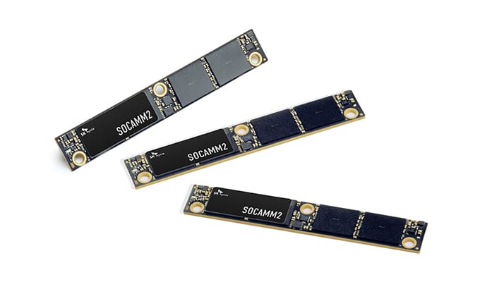
On April 19, SK Hynix announced mass production of the 192GB SOCAMM2, a next-generation server memory module on its 1cnm-process LPDDR5X. The company explicitly identified the Nvidia Vera Rubin platform as the target. Think of SOCAMM2 as scaling the power efficiency of mobile RAM up to data center density: SK Hynix says it delivers more than double the bandwidth and about 75% better power efficiency versus conventional RDIMM, per the company's announcement.
The competitive picture is three-way. SK Hynix is in production first. Micron shipped 256GB customer samples in early March — roughly 33% higher capacity relative to the 192GB SOCAMM2. Samsung is reportedly still resolving a warpage issue on its variant.
What changes if SOCAMM2 scales: AI memory becomes a tiered architecture rather than an HBM monoculture, widening the set of packaging and module suppliers who matter. What to watch: whoever wins the Vera Rubin design slot gets locked in for 18–24 months — and that makes the next two quarters of customer qualification updates more consequential than any earnings release.
TSV Complexity Is Becoming a Manufacturing Bottleneck — and Nobody's Talking About It
There's a structural problem building inside every HBM stack that the industry has been quietly managing — and it's getting harder to manage.
The culprit is the through-silicon via, or TSV — a microscopic vertical channel drilled through each die that carries signals between layers. As HBM generations advance from 8-layer to 12-layer to 16-layer stacks, the number of TSVs per die multiplies, aspect ratios get more extreme, and the yield math gets brutal: one bad TSV in a 16-die stack can scrap the entire assembly. Semiconductor Engineering reported this week that TSV complexity is now a first-order capacity constraint — not just a process challenge but a gate on how fast the industry can scale HBM output regardless of wafer starts.
The problem compounds at HBM4, where the base die moves to a logic process at TSMC, introducing a new interface between two fab ecosystems that don't naturally speak to each other.
The quiet implication: TSV drill toolmakers (Tokyo Electron, Applied Materials), copper fill systems, and CMP tool vendors are seeing demand that isn't fully visible in public WFE forecasts because it's back-end capex. Watch ASE and Amkor's next earnings calls — if they start flagging TSV-related capacity constraints, the HBM ramp story changes from "how many wafers" to "how many stacks per wafer."
TSMC's Quarter Says the AI Build-Out Still Hasn't Hit the Wall
When TSMC talks, the entire chip industry gets an X-ray. Q1 results released April 16 showed revenue of NT$1.134 trillion and net income of NT$572.5 billion — both records — with capital spending nudged toward the high end of the prior range.
The useful bit is the mix, not the totals. Advanced nodes kept taking a larger share, which tells you the capacity squeeze remains concentrated where the most valuable compute lives: 3nm and below on the front end, advanced packaging behind it. TSMC also warned that the Iran conflict could disrupt supplies of critical gases and chemicals — a reminder that materials are still a first-order constraint.
Separately, regional reporting says TSMC has set aside NT$20 billion (about $620 million) for a bonus pool and is planning raises of up to 9% for senior engineers this year. Retention is now part of capex execution risk.
The signal to watch: April monthly revenue, due in early May, will be the first post-Section 232-probe data point. Any sequential softness would more likely indicate customer caution than demand destruction — and those two things look identical in a headline.
BIS Hits Cadence with $95M Penalty for EDA Exports — and the Legal Theory Is the Story
The Bureau of Industry and Security imposed a $95 million administrative penalty against Cadence Design Systems for illegal EDA exports to Entity List parties, alongside a concurrent $45 million DOJ forfeiture. It's the largest EDA enforcement action on record — and the details matter more than the dollar figure.
Per the BIS settlement, the settlement states that employees of Cadence's Chinese subsidiary knowingly transferred sensitive U.S. technology. The settlement says Cadence assigned contracts with a restricted party to Phytium while knowing or having reason to know that Phytium and the original restricted party were closely linked through overlapping personnel.
The enforcement theory: BIS is treating EDA transfers to subsidiary employees as equivalent to direct exports to restricted entities. That's a meaningful expansion in practice, not just on paper. For any EDA vendor with Chinese subsidiary operations — Synopsys, Siemens EDA, Ansys — this case rewrites the compliance calculus. BIS has moved up the design stack: first chips, then packaging substrates, now the software that designs the chips.
The observable signal of how seriously the rest of the industry takes this: watch for quiet reorganizations of Chinese subsidiary engineering workflows over the next 60 days. If they don't happen, the next penalty will likely be larger.
ASML Raises Guidance — Which Is Really a Forecast for Everyone Else's Fab Spending
ASML lifted its 2026 revenue outlook after stronger-than-expected Q1 results, saying AI demand is driving more orders for its lithography systems. Why should a packaging engineer or OEM procurement team care? Because ASML sits so far upstream that its order book tells you what fabs are planning before those decisions show up elsewhere. Chipmakers reserving expensive lithography tools with multi-quarter lead times are not behaving like companies expecting an AI pause.
The geographic angle matters too: ASML's China exposure remains unusually high, which means export-control policy and customer qualification are now mixed into the same earnings discussion as pure technology demand.
What to watch: whether Tokyo Electron, Lam, and KLA echo ASML's raised outlook in the next round of commentary, or draw sharper regional lines around where growth is coming from. If they echo it, expect upstream materials and service markets to tighten — longer lead times and higher spot prices for specialty chemicals and gases. If they don't, ASML's China number is carrying more of the story than the AI narrative admits.
⚡ What Most People Missed
- NAND and DRAM spot prices are quietly drifting lower even as contract prices are guided up 60–75% for Q2. TrendForce's April 15 update shows DDR4 spot falling 0.48% as of April 15 while suppliers try — and fail — to lift NAND spot prices to validate the contract surge. Some spot traders have begun liquidating inventory to capture arbitrage. If spot doesn't track contracts upward within 4–6 weeks, the narrative that Q2 gains are hyperscaler-only becomes much stronger.
- Chinese fabs are importing record volumes of U.S. chipmaking equipment via Singapore and Malaysia, per a line buried in Tom's Hardware reporting this week. The timing — nine days after the April 13 BIS deadline tightening IC designer approvals — is notable. Per the Congressional Research Service, Changxin Memory Technologies, a lead in China's HBM push, remains unlisted and can still purchase U.S. equipment directly.
- ABF substrate supply is tightening again — and this time the squeeze is upstream of CoWoS. DigiTimes reported April 9 that larger AI GPU dies and higher layer counts are eating substrate capacity faster than unit growth suggests. If CoWoS was last year's obvious choke point, ABF looks like the less visible one a layer underneath.
- A former Samsung researcher was sentenced to seven years in prison this week for transferring core semiconductor technology to China, confirmed by KBS News, JoongAng Daily, and Chosunbiz. It's the stiffest sentence yet in a Korean semiconductor IP case and a deliberate signal that Korean courts now treat chip espionage as national security, not corporate crime.
- A cost-reduced DDR5 variant is surfacing in developer benchmarks. Early developer tests posted on Reddit show roughly a 50% throughput reduction on a single subchannel. Treat this as a Tier 3 signal, not confirmed product data — but if the format scales into mainstream channels, it's evidence that DRAM pricing pressure is forcing architectural compromises in lower-tier servers and desktops.
- China's Baiyi Time Space confirmed mass production of domestic KrF photoresist resins — the light-sensitive chemicals for older-generation lithography, with a reserve of hundreds of tons. KrF resists are used at 28nm and above, exactly where China's domestic capacity is concentrated. Another quiet localization data point.
📅 What to Watch
- If Samsung Q1 earnings on April 23 include vague HBM3E qualification language, the Nvidia supply relationship may still be at risk — and that would widen SK Hynix's structural lead by a full product generation.
- If 30,000+ workers show up at Pyeongtaek on April 23 and management makes no concession, expect DRAM and NAND spot prices to move within a week on precautionary buyer orders, well before any actual stoppage.
- If spot memory prices don't begin tracking contracts upward by late May, the Q2 contract surge is likely a hyperscaler-allocation story rather than a broad market recovery — which would mean OEMs and industrial buyers defer new purchases, extending inventory gluts into H2.
- If Tokyo Electron, Lam, or KLA echo ASML's raised outlook, specialty gases and photoresists are likely to tighten in the following months — and helium procurement could become a competitive advantage rather than a routine line item.
- If Air Liquide or Linde declare force majeure on helium delivery contracts, that would be a hard cap on front-end throughput at leading-edge logic fabs globally.
- If Samsung or Micron announce dedicated HBM packaging facilities in the next two quarters, SK Hynix's P&T7 bet becomes a race, not a moat.
The Closer
This week: 40,000 Samsung workers massing at Pyeongtaek over bonus envelopes a third the size of their neighbors', Cadence employees in a Shanghai office quietly reassigning contracts to a company with the same people at a different front door, and concrete drying in Cheongju for a building that doesn't exist yet but whose output is already sold. The AI boom has produced its first genuinely surreal artifact: a memory market where contract prices scream up 75% while spot prices drift down and no one can quite explain who's right — except the spot traders liquidating inventory for cash, who apparently have an opinion. See you next week.
Forward this to the procurement lead who still thinks HBM is a wafer problem.